×
SAVE TIME. TAKE A BREAK

When you need the most efficient and effective measurement devices for semiconductor tool set-up and maintenance processes, count on CyberOptics, the global market leader in wireless semiconductor measurement devices for chamber gapping, leveling, wafer handoff teaching, vibration, airborne particle, relative humidity and resistance measurement.

Semiconductor fabs and OEMs value the accuracy, precision and versatility of the WaferSense and ReticleSense measurement portfolio to enable improvements in fab yields and equipment uptime.


Save Time & Expense

  • Improve yields and increase tool uptime
  • Increase throughput
  • Reduce resource needs
  • Speed equipment set-up, maintenance cycles, trouble-shooting, qualification and release to production
  • Speed tool optimization, stabilization and standardization
  • Streamline fab processes
  • Establish repeatable and verifiable standards

Most Efficient and Effective

Since the wireless, Bluetooth® enabled and battery powered devices are wafer or reticle shaped, they can generally travel anywhere a wafer or reticle travels, providing optimal ease-of-use and access to locations that otherwise may be difficult or impossible to reach.

Vacuum Compatible

Calibrations can be done under closed-chamber process conditions with the vacuum compatible WaferSense and ReticleSense measurement devices.

Intuitive Software

Receive and record data in real-time on your laptop with CyberOptics easy-to-use software and count on accurate, precise, reliable and repeatable results that save time and expense compared to traditional or legacy methods.

Application:
Type:

ReticleSense® Auto Teaching System™ (ATSR)

ATSR
  • Quickly teaches accurate wafer and reticle hand-off calibration for proper alignment and set-up of semiconductor tools.
  • “Sees” inside the tools to capture three dimensional off-set data (x, y and z) in real-time to quickly teach wafer and reticle transfer positions – all without opening the tools.
  • Conduct repeatable and reproducible setups and maintenance checks, speed trouble-shooting and eliminate technician-to-technician variation.
  • Includes CyberSpectrum™ software.

WaferSense® Auto Teaching System™ (ATS2)

ATS
  • Improve yields and lower particulate contamination with accurate wafer handoff calibration.
  • Achieve repeatable and reproducible semiconductor equipment setups.
  • Reduce equipment downtime from hours to minutes.
  • Speed trouble-shooting and lower consumable expense with visual inspection.

WaferSense® Auto Resistance Sensor™ (ARS)

ARS
  • Shorten equipment maintenance cycles with wafer-like 4-wire resistance sensor.
  • Predict when a tool needs maintenance with quantitative analysis of measured mean resistance over time.
  • Improve cell-to-cell process uniformity with objective and repeatable resistance measurement.
  • Includes CyberSpectrum™ software.

WaferSense® Auto Vibration and Leveling Sensor™ (AVLS3)

AVLS3
  • Speed equipment qualification with wireless measurements.
  • Shorten equipment maintenance cycles with thin and lightweight wafer-like form factor.
  • Lower equipment maintenance expenses and enhance process uniformity with objectiv eand reproducible data.
  • Includes CyberSpectrum™ Software

WaferSense® Airborne Particle Sensor™

APS1, 2 & 3
  • Quickly monitors, identifies and enables troubleshooting of airborne particles down to 0.14um within semiconductor process equipment and automated material handling systems.
  • Easily identifies when and where the particles originate and measures the effectiveness of cleaning adjustments and repairs in real-time.
  • Includes CyberSpectrum™ software.

WaferSense® Auto Multi Sensor™

AMS
  • Speed equipment qualification with wireless measurements.
  • Shorten equipment maintenance cycles with thin and lightweight wafer-like form factor.
  • Lower equipment maintenance expenses and enhance process uniformity with objective and reproducible data.
  • Includes CyberSpectrum™ software.

WaferSense® Auto Gapping System™ (AGS)

AGS
  • Speeds non-contact gap measurements and parallelism adjustments under
    vacuum for semiconductor processes such as thin-film deposition, sputtering and etch.
  • Improves uniformity, tool availability and repeatability.
  • Includes CyberSpectrum™ software.

WaferSense® Auto Vibration System™ (AVS)

AVS
  • Monitors 3-axis accelerations and vibration to enable yield improvements by maximizing acceleration and minimizing vibration.
  • Records vibration data for easy comparison between past and present, as well as one tool to another, to reduce particles, maintenance time and cycle time.
  • Includes CyberSpectrum™ software.

WaferSense® Auto Leveling System 2 Vertical™ (ALS/ALS2V)

ALS2V
  • Speeds setting the right inclination by measuring pitch, roll, rise overrun and vertical inclinations.
  • Quickly and accurately enables setting the same level across the tools for better process uniformity.
  • Includes CyberSpectrum™ software.

ReticleSense® Airborne Particle Sensor™ (APSR/APSRQ)

APSR / APSRQ
  • Quickly monitors, identifies and enables troubleshooting of airborne particles down to
    0.14um within semiconductor process equipment and
    automated material handling systems.
  • Easily identifies when and where the particles originate
    and measures the effectiveness of cleaning adjustments and repairs in real-time.
  • Includes CyberSpectrum™ software.

ReticleSense® Auto Multi Sensor™ (AMSR)

AMSR
  • Speed equipment qualification with wireless measurements.
  • Shorten equipment maintenance cycles with reticle-like form factor.
  • Lower equipment maintenance expenses and enhance process uniformity with objective and reproducible data.
  • Includes CyberSpectrum™ software.

In-line Particle Sensor™ (IPS™)

IPS
  • Speed equipment qualification with real-time 24/7 monitoring.
  • Shorten equipment maintenance cycles with inline particle sensing.
  • Lower equipment expenses with objective and reproducible data.
  • Includes CyberSpectrum™ software.

CyberSpectrum™ Software

SOFTWARE FOR WAFERSENSE® • RETICLESENSE® • In-Line Particle Sensor™

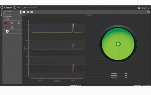
CyberSpectrum is a powerful yet extremely simple software with an intuitive interface providing numerical and visual feedback for real-time measurement and analysis for multiple applications.

WaferSense® SDK

SOFTWARE DEVELOPMENT KIT

The WaferSense Software Development Kit provides the Application Programming Interface (API) to the WaferSense® and ReticleSense® family of devices. This allows direct integration of the device into user developed software applications.

NanoResolution MRS® Sensor

Powered by MRS® Technology

NanoResolution MRS Sensor for Wafer-Level and Advanced Packaging Applications for OEM integration.

SQ3000 CMM for Semiconductor Applications

The Ultimate in Speed and Accuracy for Coordinate Measurement Applications - Seconds. Not Hours

EX-Q Wafer Mapping Sensor

A DRAMATIC STEP FORWARD IN WAFER DETECTION

EX-QS Wafer Mapping Sensor

GOOD THINGS DO COME IN SMALL PACKAGES

Digital and Analog Frame Grabbers

DEPENDABLE, QUICK SETUP MACHINE VISION COMPONENTS