Powered by MRS® Technology
WX3000™ Metrology and Inspection Systems for Wafer-Level and Advanced Packaging
Make an Inquiry
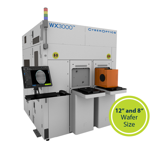
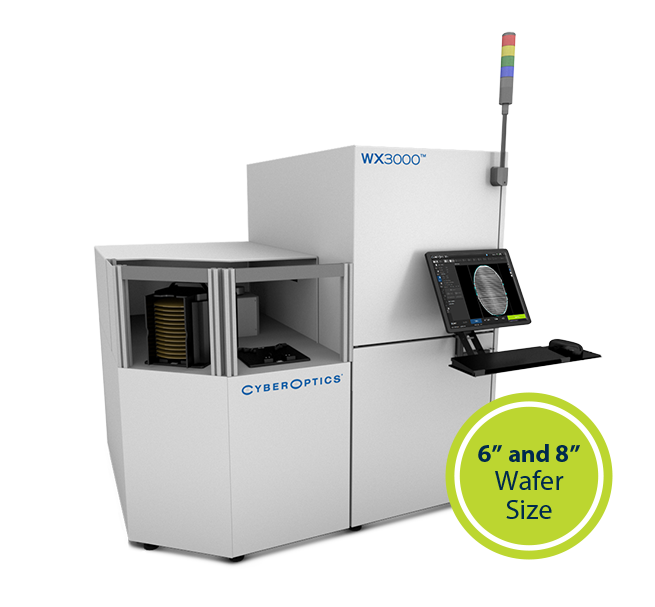

WX3000 3D and 2D metrology and inspection system provides the ultimate combination of high speed, high resolution and high accuracy for wafer-level and advanced packaging applications to improve yields and productivity. Powered by Multi-Reflection Suppression® (MRS®) Sensor Technology.
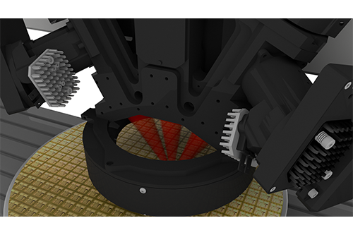
Metrology-Grade Accuracy with MRS® Technology ![]()
Fast, Superior Inspection Performance ![]()
Versatility for Wafer-Level and Advanced Packaging Applications ![]()
The 3-micron NanoResolution (X/Y resolution of 3
micron, Z resolution of 50 nanometer) MRS sensor
enables metrology grade accuracy with superior 100% 3D and 2D measurement performance for features as small as 25-micron.
100% 3D and 2D metrology and
inspection can be completed simultaneously at high
speed, versus an alternate, slow method that requires
two separate scans for 2D and 3D, and only a sampling
of a few die.
Delivering greater than 25 wafers (300mm) per hour for 12″ and 8″ wafer sizes and 55 wafers per hour (200mm) for 6″ and 8″ wafer sizes.

3D Capability
Full Wafer
3D Accuracy
0.2μm (VLSI standard)
3D Repeatability
0.3 µm @ 3σ (VLSI standard)
Bump Height (Size) Coverage Range
25-250 μm
3D + 2D Throughput (300mm full wafer)
≥ 25 WPH
3D + 2D Throughput (200mm full wafer)
≥ 55 WPH
2D Objectives and Resolution
Fixed resolution – 3μm
2D Measurement Accuracy for Bump & RDL
1/2 (1.5μm) pixel size accuracy
2D Measurement Repeatability
1.6μm @ 3σ
2D Measurement Range
>20μm
See brochures for additional specifications


