Powered by MRS® Technology

NanoResolution MRS® Sensor

Make an Inquiry
Make an Inquiry

Offering an unparalleled combination of high accuracy, high resolution and speed, MRS® sensors are widely used for inspection and measurement in the SMT and semiconductor markets.

Metrology-Grade Accuracy with MRS® Technology

Sub-micrometer accuracy for features as small as 25 μm

Accurately inspect shiny or mirror-like surfaces with sensor technology that rejects spurious reflections.

Attain repeatable and reproducible measurements.

Fast, Superior Inspection Performance

Increase throughput with the MRS sensor that is 2-3X faster, delivering greater than 25 wafers (300mm) per hour.

Conduct 100% 3D and 2D metrology and inspection versus sampling-only methods.

Attain 3D and 2D measurements in one pass vs. multiple separate scans.

Versatility for Mid-End and Advanced Packaging Applications

Measure and inspect a wide range of applications including solder balls and bumps, wafer bumps, copper pillars and other mid-end and advanced packaging applications.

Achieve high speed, highly accurate, 3D and 2D metrology and inspection for critical packaging features including bump height, coplanarity, diameter and shape, relative location and variety of other measurements.

Fast, Superior Inspection Performance

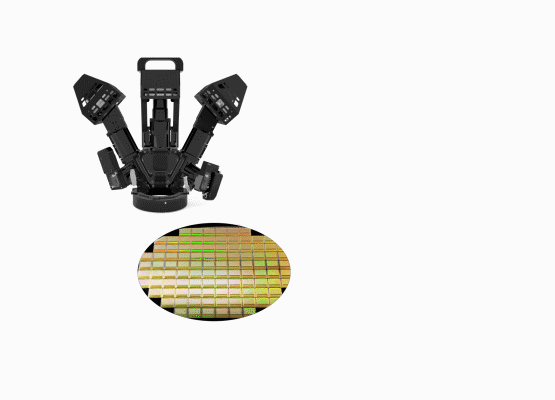
Increase throughput with the MRS® sensor that is 2-3X faster, delivering greater than 25 wafers (300mm) per
hour.

Minimum Feature Diameter

25 µm

FOV

15×15 mm

Lateral Resolution

3 µm

3D Sensor Height Resolution

0.05 µm

3D Repeatability

0.3 µm @ 3σ (VLSI standard)

3D Accuracy

0.2 µm (VLSI standard)

Height Measurement Range

0.25 mm

3D Acquisition Time, typical

150 msec

Illumination

Integrated 2D Illumination