 Back to News
Ahead of the Curve: The Future of 3D Optical Inspection
As published in US Tech | By Dr. Subodh Kulkarni, President and CEO, CyberOptics Corp.
Demand for speed and accuracy in inspection is continually growing in the electronics industry, but incremental progress in camera and projector setups is not a long-term solution. New multifunctional sensors that can be applied to a broader range of 3D optical inspection and measurement application are raising the bar for the electronics and semiconductor markets.
CyberOptics’ customers span a variety of different vertical sectors, from consumer electronics to aerospace, automotive and medical devices. The needs of these different customers are actually quite similar, whether it be for automated optical inspection (AOI), solder-based inspection, semiconductor inspection, or parts inspection. In each case, the customer is looking to improve operating efficiencies, production yields and quality.
As a company, CyberOptics develops and manufactures high-precision 3D sensors for the industrial metrology, SMT and semiconductor markets. The company’s proprietary, advanced sensor technology sharpens the customer’s competitive edge as the demand rises for higher accuracy at faster production speeds.
Key Market Drivers
In the SMT market, main drivers include the decrease in size of electronics packaging and the increase in density of PCBs, challenges from tall components near very small components, and complex applications. There is definitely a greater need for precision, accuracy and speed that continues to shift the market toward 3D optical inspection.
We are seeing more and more challenging applications from customers in SMT, semiconductor and industrial metrology, where CyberOptics has successfully demonstrated capabilities far beyond those of its competitors.
CyberOptics’ 3D multiple reflection suppression (MRS) sensor technology has proven effective for flux inspection, wirebond inspection, die-attach applications, shiny flip chip packaging, microelectronics, sub-100-micron solder paste deposits, very small LEDs, micro-LEDs, paste printing onto chip products, socket metrology, molded parts inspection, and various other complex applications.
MRS is a technology that enables metrology-grade accuracy by inhibiting optical measurement distortions and reflections. Essentially, it digitally “tags” the light to ensure that multiple reflections are suppressed, allowing high-quality measurement and inspection.
This is vastly different from what our competitors are doing. Their systems typically comprise a single camera and multiple projectors in series, but CyberOptics’ solution reverses that by incorporating multiple cameras and a digital projector. The secret sauce, however, is really the algorithms.
The fact that MRS technology is now at the heart of the world’s smartphone manufacturing inspection and increasingly used in various applications where high accuracy and speed are vital, underscores its importance.
CyberOptics has been pioneering optical sensing technology for three decades, due to its sensor expertise, sophisticated algorithms, rich patent portfolio, and continuous advancement. Its core technology, MRS sensors, enable microscopic-level inspection at production speeds and are deployed in all target market segments.
The company has invested a great deal in this technology and believes that it is a class apart when compared with alternative technologies. Customers value the significant advantages and benefits to their yields and productivity.
Coordinate Measurement
Demand is growing for fast, accurate, x, y and z measurements of circuits and devices. This is the case regardless of whether the manufacturer is building PCBs, semiconductors or consumer electronics.
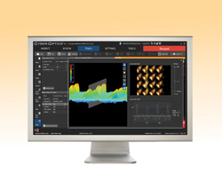
CyberOptics’ SQ3000™ coordinate measurement machine (CMM), an extension of the company’s SQ3000 AOI system, was developed in close consultation with customers. This machine can measure any object and deliver hundreds of thousands of dimensions simultaneously in less than 10 seconds. Traditional CMMs are invariably less accurate, far more complicated to use and usually take hours to measure.
Many customers making high-end products are asking for more measurement capabilities. It is no longer sufficient to say whether a part is good or bad from a simple pass/fail inspection report. Customers need to know why and how. Once that is determined, it is easy to feed back the data to quickly identify the initial problem and eliminate subsequent defects. Measurement, as well as inspection, is vital to the smart factory.
Ultimately, the quicker the manufacturer can obtain measurements, the faster he or she can analyze it, make the necessary changes and continue production. Customers are also looking for multifunctional capability — AOI, SPI and coordinate measurement.
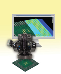
CyberOptics’ CMM excels at socket metrology, measuring thousands of pins in around 10 seconds.
In socket metrology, there are thousands of pins on a circuit board and before the CPU or GPU is mounted, it is critical to ensure that all of the pins have the correct heights, dimensions and angles. Typical coordinate measurement involves sampling pins, which takes hours, is not accurate enough, and does not provide 100 percent inspection. With MRS sensor technology deployed for coordinate measurement, inspection of the thousands of pins can be accomplished in less than 10 or 15 seconds.
Semiconductor Market
In the semiconductor market, MRS sensors are currently being used in KLA-Tencor’s backend packaging inspection systems. There is also a significant opportunity to leverage the sensor’s combination of speed and accuracy in applications in the mid-end, where its advantages have been demonstrated.
CyberOptics’ ultra-high-resolution MRS sensors have been shown to be highly effective for IC packaging, wafer bump inspection and mid-end semiconductor applications, where it delivers a high degree of accuracy and precision, with a significant speed advantage. The company sees potential in the frontend semi market for MRS, where CyberOptics currently offers its WaferSense and ReticleSense wireless measurement devices for semiconductor tool applications.
In the future, we will see a continued merging of the SMT and semiconductor markets, due to the growing area of advanced electronic packaging. The latest smartphones, such as the iPhone X or Samsung Note S9, are good examples. Instead of incorporating a traditional PCB, these devices typically house an advanced package developed by Apple or Samsung.
We are likely to see the PCB industry change dramatically for these kinds of advanced packages, where accurate measurement is vital to ensure that yields are high. As the number of advanced products continues to grow, established providers that reach across SMT, semiconductor and metrology industry segments have a great opportunity.


