 Back to News
The Convergence of the Semiconductor and SMT Markets
As published in US Tech | By Dr. Subodh Kulkarni, President and CEO, CyberOptics Corp.
The Growing Need to Identify Critical Defects and Measure Critical Parameters

There is a confluence of factors leading the back-end of semiconductor and SMT industries to start merging, and very high-end electronics and semiconductors are driving a lot of this. Stacking of chips, components getting smaller, silicon surfaces and reflective components are all beginning to play a role now in electronics.
The exciting aspect from my viewpoint is whether it’s the fortune 100 companies, the high-end smartphone companies, the high-end electronics manufacturing companies or the semiconductor fabs, they are not happy with any solutions that are available today, so the need is there. There is an urgent issue right now and neither the semiconductor industry, nor the SMT industry has been able to solve those problems today, so that is why I view this is as fertile ground for those of us who can address these challenges.
Inspection and Measurement
Customers want more than inspection and a pass/fail report. What they really need to know is point-to-point distance, line-to-line distance, and they are really asking questions that historically the electronics industry or even the back-end of semiconductor industry previously had not asked. Now they are seeking XYZ measurements and determining what it means for their process if the measurement is not right. They are considering what they feed back to their process and how they can control their process better.
This presents opportunities for the advanced companies with advanced technologies, which is where CyberOptics thrives. The industry dynamics are creating a real need for highly accurate 3D measurements, not just optical inspections, but optical measurements at high speeds as well. This is where CyberOptics proprietary 3D Multi-Reflection Suppression (MRS) sensor technology is highly valued. It is faster and more accurate than any other 3D conventional technology and mitigates reflection-based measurement distortions for metrology-grade image quality. Customers continue to come to us because they need speed, they need accuracy and they need resolution. They need the best combination of these attributes for their applications.
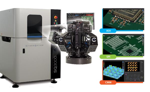
Customers worldwide have been rapidly adopting the 3D MRS-Enabled SQ3000™ Multi-Function system for AOI, SPI and CMM (Coordinate Measurements) and recognize it as the premier process control solution, particularly for the most challenging applications. The multi-function system can identify critical defects and measure critical parameters, in order to fix what can be found and control what can be measured. Ultimately, we are enabling significant improvements in yields, quality and operational efficiencies in their manufacturing facilities.
Proprietary Sensor Technology Fueling Company Growth
CyberOptics’ 2018 overall revenues increased 21% over 2017. Fourth quarter 2018 sales of inspection and metrology systems increased 46% year-over-year. Within this category, sales of 3D MRS-enabled SQ3000 automated optical inspection or AOI systems, including the SQ3000 CMM that incorporates AOI with metrology functionality, rose 40% year-over-year in the fourth quarter driven by the competitive advantages of the MRS technology platform.
With our rich patent portfolio and key technology platforms addressing challenging applications across these markets – SMT, semiconductor and industrial metrology, we believe CyberOptics is well positioned for continued solid growth and profitability in the next three to five years.
MRS-Enabled Systems Delivering Significant Growth
MRS technology has enabled us to strengthen our position in existing SMT markets and participate in the back-end semiconductor market, where our MRS sensors are integrated into KLA®’s back-end inspection systems. We have further extended the technology into the mid-end semiconductor market where we see a large growth opportunity in advanced packaging.
MRS sensors can measure cracks and defects as small as 30 microns which is important as electronics packaging continues to shrink, components are more densely combined on circuit boards, tall components are near small components and the various stacking technologies in the rapidly growing advanced packaging market – all driving the need for high-precision inspection and measurement.
Mid-End Semiconductor and Advanced Packaging
There are various definitions in the market, but features that are larger than 100 microns we typically see in the back-end semiconductor area. Features that are sub 10 micron, we typically see in the front-end area and everything in the middle is generally referred to as the broad, mid-end area.
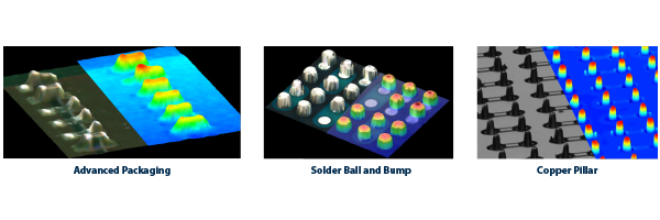
There is a plethora of activity in the mid-end and advanced packaging market whether it is wire bonding, stacked die, Cu pillars or C4 solder bumps. Advanced Packaging where dies are integrating vertically involve finer features with more layers and I/Os. There are various stacking technologies. Whether it is fan-in or fan-out where the packaging of the dies is done while still on the wafer, embedded die, or TSVs (Through silicon via), it is clear there is a growing need to effectively identify and control defects.
The mid-end and advanced packaging market is growing very fast. According to Yole Développement, the advanced packaging market revenue is projected to grow from around $28 billion in 2019 to around $33 billion in 2022. With all of the complexity, variations of packaging types and continued advancements, yield challenges are increasing. Right now, the industry wants high accuracy, high resolution and higher speed for 100% inspection. Volumes are increasing in this area because of stacking and other advanced packaging applications, so speed is a critical factor right now.
MRS Sensor Technology Advancements
In 2015, when we launched the MRS technology our pixel was eighteen micron. From eighteen microns, we have come down to three microns. In four years, we have roughly advanced by a factor of six. In addition, our 3-micron 3D MRS sensor is capable of handling specular surfaces, so in addition to a factor of 6 improvement in resolution in the last 4 years, we have added the ability to handle mirror like surfaces.
CyberOptics’ latest MRS sensor is ideal for the mid-end inspection area. Typically, there is a factor of 10 to 1 – with our 3-micron 3D sensor we can deliver high-precision accuracy and resolution for features that are 30 micron or above. The big differentiator is the high resolution and accuracy that the industry needs, and our speed advantage – our MRS sensor technology is 2-3X faster than alternate solutions in the marketplace.
Going forward we will continue to advance our sensor technology with various levers, including improvements in pixel size and further advancements in our proprietary MRS algorithms – our secret sauce. In the future, we anticipate delivering sub-one micron resolution for features that are sub-five micron to start approaching the front-end semiconductor area.
Note: KLA is a registered trademark of KLA Corporation.


