 Back to News
Merging of Two Markets: SMT & Semiconductor
As published in Global SMT & Packaging – June 2019 | By Dr. Subodh Kulkarni, President and CEO, CyberOptics Corp.

Complexity Drives the Need for Effective Inspection and Measurement
The lines are blurring between the SMT and semiconductor industries. Driven by high-end electronics and semiconductors, the need to identify critical defects and measure critical parameters continues to increase. There are various challenges whether it is tall components next to small components, components getting smaller or shiny reflective surfaces.
The semiconductor packaging industry continues to advance with a trend in higher density and higher integration, more layers, finer features and more I/O channels. This is driven in part by a requirement for higher bandwidth and lower power consumption. There are various advanced packaging configurations such as 2.5D and 3D stacking technologies with or without through silicon via (TSV), emerging technologies and shiny silicon surfaces to contend with. With this increase in complexity, various packaging options and continued innovation, yield challenges are increasing.
Both SMT and semiconductor industries have a need for 100% inspection and measurement to detect defects and improve process control, particularly for the high-end segment. This is fertile ground for high-precision sensing solutions that can deliver the needed combination of accuracy, resolution and speed.
Process Control Becomes Even More Vital
Customers are seeking XYZ measurements and determining what it means for their process if the measurement is not accurate. It is no longer just inspection and a pass/fail report. Controlling their process has become even more important for effective yield management.
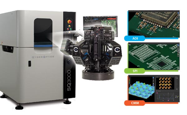
This growing need continues to fuel the rapid adoption of our 3D MRS-Enabled SQ3000™ Multi-Function system for AOI, SPI and CMM (Coordinate Measurements) as the premier process control solution, particularly for the most challenging applications. Garnering twelve industry awards to date, this all-in-one system can identify critical defects and measure critical parameters to improve yields, quality and operational efficiencies in manufacturing facilities.
Combination of Attributes Drives MRS Technology Adoption
Customers require high accuracy, resolution and speed, especially for the high-end applications. Our proprietary 3D MRS sensor technology delivers on all three requirements. It is faster and more accurate than any other 3D conventional technology. It offers a distinct advantage in the market with its sophisticated fusing algorithms and ability to mitigate reflection-based measurement distortions for metrology-grade image quality.
MRS technology is in use at over 100 customers worldwide and continues to drive significant revenue growth for CyberOptics. We anticipate ongoing rapid adoption based on the competitive advantages of the MRS technology platform, particularly for challenging applications where our technology really shines.
Mid-End Semiconductor Is a High Growth Market
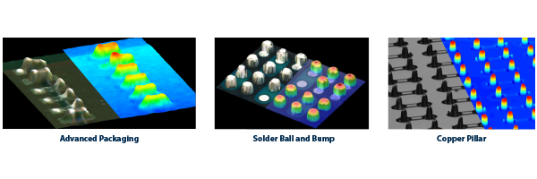
In the semiconductor landscape, we view the mid-end to be in between the front-end, where features are sub one micron, and the back-end, where features are typically greater than 100 microns. Yole Développement projects the advanced packaging market in mid-end, to grow from around $28 billion to approximately $33 billion by 2022. Within this market, there are flip-chip (FC), fan-in (FI), fan-out (FO), embedded die (ED) and TSV, all ripe for highly accurate 100% inspection. Stacked die, wire bonding, Cu pillars and C4 solder balls and bumps are some of the key applications.
Proprietary MRS Technology Extends to Mid-End Semi and Advanced Packaging
Designed for the mid-end inspection area, our new ultra high-resolution three-micron 3D sensor delivers sub-micrometer accuracy that the industry needs for features that are as small as twenty-five micron. When we first introduced the MRS sensor technology in 2015, our pixel was eighteen micron. Since launch, in the last four years, we have advanced by a factor of six.
We also have added the ability to handle mirror-like surfaces. While retaining its ability to reject spurious multiple reflections, the sensor can capture and analyze specular reflections from shiny surfaces of solder balls, bumps and pillars, enabling accurate inspection and 3D metrology of these critical packaging features.
In addition, it is two to three times faster than alternate solutions in the marketplace. With data processing speeds in excess of seventy five million 3D points per second, it delivers throughput greater than twenty-five wafers (300mm) per hour.
Continued R&D Investment
MRS sensor technology is used in all three of our target segments – SMT, semiconductor and industrial metrology. In the semiconductor back-end area, our sensors are integrated into KLA®’s BEOL systems. In semiconductor mid-end / advanced packaging area, our new three-micron sensor is ideal. In the future, we are aiming to deliver sub-one micron resolution for features that are sub-five micron to enter the front-end semiconductor area.
With continued investment in R&D, we will continue to advance the MRS technology including pixel size and further advancements of our proprietary MRS algorithms – our secret sauce that provides a solid and distinct competitive barrier.
Note: KLA is a registered trademark of KLA Corporation.


