 Back to News
CyberOptics Featured in Manufacturing Today
As published in Manufacturing Today Volume 19, Issue 2A. “Passing Inspection. New Optical Sensor Technology has enabled CyberOptics Corporation to Grow.”| Mark Lawton. Read full article at Manufacturing Today

In a recent article published on Manufacturing Today, Jeff Bertelsen – CyberOptics COO and CFO, provided insight into the developments and advancements in 3D optical sensor technology that has enabled CyberOptics to grow in key market segments.
CyberOptics Corporation designs, develops and manufactures high precision optical sensors and systems for inspection and measurement in the surface mount technology (SMT), semiconductor and industrial metrology markets. Its equipment is used in manufacturing environments to improve yields, throughput, quality, productivity, processes and operational efficiencies.
The majority of its customers are large semiconductor manufacturers including Intel, Samsung and TSMC, semiconductor equipment OEMs, memory manufacturers, and various surface mount technology / electronic assembly manufacturers focused on consumer electronics, automotive, and other vertical markets.
CyberOptics is headquartered in Minnesota, where it assembles its 2D and 3D optical sensors and WaferSense® semiconductor sensors. Its Singapore facility assembles the inspection and measurement systems, including their flagship MRS-Enabled 3D SQ3000™. It has a global footprint with offices in the United States, Europe, China and Singapore and a wide network of channel partners, representatives and distributors worldwide.
CyberOptics was founded in 1984 by Steven K. Case, a professor of optics and physics at the University of Minnesota. The company went public in 1987 and started being traded on NASDAQ in the early 1990s. “The company was originally focused on lasers and 2D optical sensors for SMT applications then we shifted our focus to 3D,” Bertelsen explains. “Surface mount technology is a method of producing electronic circuits in which the components are mounted directly onto the surface of a printed circuit board.”
Far Superior
The company is most proud of its proprietary, high-resolution multi-reflection suppression (MRS) sensor technology – a unique, advanced 3D sensing technology. “In any 3D sensing, one of the key problems for inspection and measurement accuracy is light reflection from shiny components and surfaces,” Bertelsen says. “Scientists at CyberOptics developed the MRS technology that effectively suppresses reflections to mitigate measurement distortions. The MRS technology is key to ensure we provide the most accurate images and inspection data,” Bertelsen says. “It is far superior to alternatives in the market. Our sensors are more accurate and faster than the competition.” Not only does the MRS technology inhibit reflections, it provide microscopic-quality images at production-line speeds.
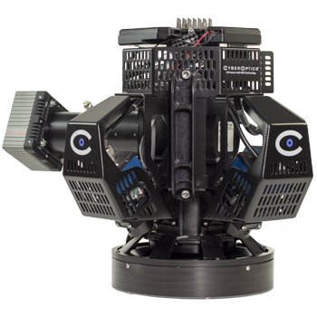
For example, take standard coordinated measurement inspection of socket pins. “It takes hours, is not accurate enough and does not provide 100 percent inspection,” Bertelsen says. “With MRS sensor technology, 100 percent inspection of thousands of pins can be accomplished in less than 10 seconds.” CyberOptics incorporates the MRS sensors in its own systems. The SQ3000™ provides multi-function capability so it can be used for automated optical inspection (AOI), solder paste inspection (SPI) and coordinated measurement (CMM). In addition to PCB inspection, it can be used to inspect and measure cell phone cases and frames, various machined and molded parts and used in various semiconductor applications.
It can measure cracks and defects as small as 30 microns. That’s important as electronics packaging continues to shrink and components are more densely combined on circuit boards and the growth in advanced packaging.
CyberOptics also has OEM agreements with some manufacturers that integrate its sensors into their equipment
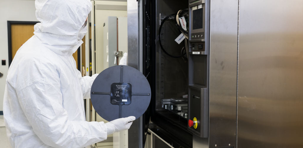
The company also produces WaferSense® wireless set-up and diagnostics sensors used in semiconductor fabrication equipment in fabs. “It helps engineers take measurements in real-time for effective tools set-up and maintenance processes,” Bertelsen explains. They’re used for chamber gapping, robot teaching, relative humidity, airborne particles, leveling and vibration applications.
Disruptive Technologies
CyberOptics has received technology and innovation awards for its MRS-enabled systems and the sales growth is impressive. “We are getting really good traction in the market. Fourth quarter sales of MRS-Enabled products rose 61% year-over-year.” Bertelsen says. “I think it is due to the disruptive nature of the MRS technology and strong differentiation. It offers an unmatched combination of speed, accuracy and resolution.” CyberOptics has seen growth in both its MRS and its WaferSense® products. “There is continued widespread adoption of our semiconductor sensors fueling growth. Fabs recognize the devices as the Best Known Method (BKM) for various applications.”
While increased sales are good news, they do come with their own challenges. “We have seen a lot of growth from these products,” Bertelsen says. “Some orders can be big. [A challenge is] forecasting them and making sure we have the right parts and material to meet our customer demands.”
While both the global economy and the semiconductor industry have been doing well, much of CyberOptics growth can be attributed to its continuous R&D efforts and technology leadership driven by President and CEO Dr. Subodh Kulkarni. “That’s really our core,” Bertelsen says. “The creativity of our research and development. That has continued to change and evolve. I think the pace of innovation has particularly picked up over the last five years. We are innovating quicker and becoming more disciplined at it.” That’s particularly true of its algorithm expertise. “The secret sauce is really the algorithms,” Bertelsen says. “That’s given us the competitive advantage.”
CyberOptics puts a lot of money and effort into research and development, even when there is not particularly strong market demand. “I think that’s the key to our success and why customers buy our product,” Bertelsen says. “We continue to invest in R&D, even if the economy is soft. Our markets can be quite cyclical. R&D has paid off with the MRS technology.
“Development took a few years before the first sales in 2015 and it’s continued to advance,” Bertelsen continues. “It’s allowed us to strengthen our position in existing SMT markets and enter new markets such as back-end semiconductor, where our MRS sensors are integrated into KLA’s back-end inspection systems. It’s also enabled us to extend further, most recently into mid-end semiconductor where we see a large growth opportunity in advanced packaging. It excels in high-end, challenging applications where our technology really shines and outperforms our competition,” Bertelsen says. “Twenty years ago, the company got 50 percent of its revenue from two or three customers. Now the number of customers has significantly expanded.”
CyberOptics holds 46 patents: 26 in the United States and 20 in other countries. It also has 21 pending patents. “2018 overall sales increased 21% over 2017. With our technology and growth with MRS and WaferSense® sensors, we think we are well positioned for very good growth and profitability in the next three to five years,” Bertelsen says.


