 Back to News
The Importance of Inspection and Metrology for Process Control in SMT and Semiconductor
By: Dr. Subodh Kulkarni, CyberOptics CEO (as published on US Tech)
Blurring of Lines between SMT and Semiconductor
The convergence between semiconductor and SMT is happening now, and it is called Advanced Packaging. You can find this convergence right in your pocket. Most high-end electronics, including smartphones, are using stacked advanced packages. No longer will you find a conventional PCB inside.
Advanced packaging is evolving rapidly with a variety of different processes and types. The goal is to have more power and functionality in a smaller package. Once you start stacking, you are dealing with extremely thin chips and the cost of failure can be very high, making inspection critically vital.
Advanced Packaging Requires High-Precision Inspection and Metrology
Every bump or pillar is essentially the glue between the stacks and some of the critical parameters to be controlled in these processes include bump height, position, diameter, shape and coplanarity. All are important for reliable connections, which leads to a significant and growing need for fast, accurate 3D inspection and metrology to improve yields and long-term reliability.
Among the inspection challenges, wafer-level and advanced packaging can create multiple specular reflections between shiny surfaces that can cause inaccurate height measurements. An inspection technology capable of effectively addressing this issue is vital. The industry not only needs high resolution and high accuracy, but 100% inspection at high speed, particularly in higher risk markets like automotive applications.
This is where CyberOptics’ strength lies. For the past few years, our R&D focus has been – and will remain – on our Multi-Reflection Suppression™ (MRS™) technology. This is a unique way of performing 3D non-contact optical sensing that we pioneered a few years ago that results in significantly faster and more accurate results than other conventional technologies. MRS meticulously identifies and rejects multiple reflections caused by shiny and specular surfaces. The real secret sauce is the algorithms.
This is why we are very optimistic about our NanoResolution MRS sensor for advanced packaging. For example, the bumps are approximately 30-40 microns each, and the pitch is about the same. To measure features this size accurately with good resolution, you need a 3 micron pixel resolution sensor. We have not only developed this higher resolution, but we also have added the capability to measure perfectly reflective mirror-like surfaces such as a silicon wafer because we can manage the specular angles as well. It can do highly accurate 100% 2D and 3D inspection, measuring critical features down to 25 micron at 25 (300mm) wafers per hour at 2-3X faster than alternate technologies.
Detecting Defects and Measuring Critical Parameters
CyberOptics is fundamentally a sensor technology company focused on semiconductor and SMT markets.
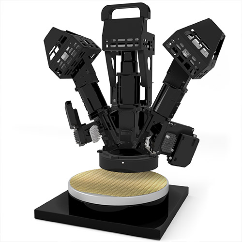
Approximately half of our customers for our flagship MRS-Enabled SQ3000™ Multi-Function systems for AOI, SPI and coordinate measurements (CMM) are using it for semiconductor applications, including advanced packaging – either the semiconductor fabs or OSATs.
The systems have been widely used in SMT applications and for other various challenging applications, particularly in the high-end segment. Because of the merging of the markets, it can be difficult to determine whether it is a semiconductor or SMT application. Regardless, given the systems can provide more than just a pass/fail report, customers are valuing the XYZ dimensions and how they can use these measurements to improve their process control.
Overall, we are enabling significant improvements in yields, quality, process control and operational efficiencies in our customers’ manufacturing facilities.
Inspection and Metrology for Micro LED technology
Another exciting growth area in the industry currently is Micro LED. We have collaborated with Rohinni, a company at the forefront in this industry. The innovation behind this flexible lighting technology is extraordinary. This disruptive technology enables products that are brighter, thinner, lighter and more dynamic than those currently on the market. Additionally, it uses less power than LCD or OLED. We believe this exciting market is well poised to grow in the coming years.
Rohinni will enable interesting commercial applications that we will see in consumer electronics devices. Micro LEDs developed using Rohinni’s technology also can be deployed in automotive applications, outdoor signage and other applications. A primary focus at this time is the backlight for LCD displays. Today, the backlight is LED. Switching to micro LED provides better power consumption and better light intensity. We have been scaling up and deploying our inspection and metrology systems for this application to maximize yields and improve processes and productivity.
Currently, Rohinni is using our systems for six critical in-line production process locations including incoming quality inspection of the flexible circuits, solder paste inspection, pre- and post-reflow AOI, coordinate measurements post-placement of the LED die, and final test.
The company selected our MRS-Enabled SQ3000 based on the unmatched performance and versatility, more specifically, the higher accuracy and higher resolution at high speed with the in-line CMM functionality.
MRS Technology Delivering Significant Growth
We continue to gain traction in the
market. Customers have been rapidly adopting our MRS-enabled technology based
on the unmatched combination of high accuracy, high resolution and high speed.
Sales of 3D MRS-enabled sensors were up 50% in the fourth quarter of 2019 on a sequential basis. Sales of sensors, inspection and metrology systems based on our 3D MRS technology rose 48% year-over-year in the fourth quarter of 2019, mainly driven by strong sales of the SQ3000 3D AOI systems.
Fourth quarter sales of inspection and metrology systems increased 83% on a quarterly sequential basis, largely driven by sales of SQ3000 systems reflecting increases of over 100% on a quarterly sequential basis and up 91% on a year-over-year basis.
Extending MRS Sensor Technology into Memory Module Applications
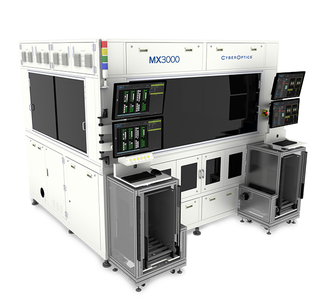
We have recently extended our portfolio of memory module inspection and metrology systems from 2D to 3D with the launch of our MX3000™ system. With two high-resolution MRS sensors, the system enables highly accurate, dual-sided final vision inspection and doubles productivity.
There are roughly 120 -130 memory lines in the world today. The majority of them are in the three large manufacturers, Samsung, SK Hynix and Micron, and there are a few others in smaller players as well. That overall number is growing at an approximate 10% run rate because of demand for memory.
MRS Sensor Technology and Semiconductor Sensors for the Front-End Pave the Way for Future Growth
To further strengthen our position in the semiconductor market, we expanded our family of semiconductor sensors with two new products. The first is the wireless WaferSense® Auto Resistance Sensor™ (ARS™) that enables real-time resistance measurements of plating cell contacts in semiconductor Electrochemical Deposition Applications for tool set-up and diagnostics.
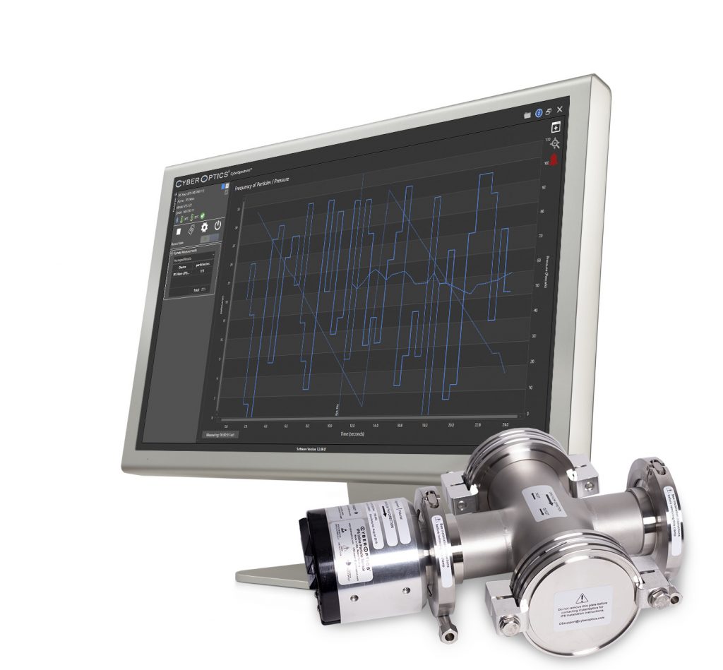
The other recent launch is the In-Line Particle Sensor™ (IPS™) that detects particle contaminant in gas and vacuum lines in semiconductor process equipment. The ability to monitor particles in-line is particularly relevant for EUV lithography tools because particle detection can improve our customers’ yield, tool uptime and productivity significantly.
Currently, there are approximately 100 EUV tools worldwide, and the number is growing by about 15% annually. Most of the tools are within three fabs right now. Over time, that number is expected to increase. Our opportunity lies in having our IPS sensor in multiple pumping lines on the EUV tool and measuring the particles, providing the process engineer with visibility when particle concentration is increasing. This could indicate that the collector efficiency could be in jeopardy, so they would perform a gas purge or flush. Today, they cannot do that without data to inform them of the issue. Based on their guess, they actually shut down the tool and perform the purges. Either they may be overdoing it or underdoing it, both of which can be problematic in terms of yield and productivity. When they have spent that much on the tool, productivity is a big issue. Anything that helps improve their yield and productivity is valuable for EUV lithography, which is what the IPS is targeted to address.
Future Growth Drivers
5G deployment, cloud and AI are a few of the key market drivers that will enable future growth in SMT, semiconductor and the converging market of Advanced Packaging. CyberOptics is well poised for growth in the coming years with our proprietary technology platforms and commitment to innovation. We aim to stay ahead of our customers’ needs and deliver significant customer benefits.


