 Back to News
Process Control Needs Are Increasing Across Semiconductor Fabs
As published in Semiconductor Digest – June 2019, pages 28 and 29 | By Dr. Subodh Kulkarni, President and CEO, CyberOptics Corp.
Whether for diagnostics, qualification or preventive maintenance, equipment engineers in the fab need to adjust their tools. However, there are several limitations in the fab environment for attaining the measurements that determine the needed adjustments. Legacy methods can be cumbersome, non-representative and they do not provide data in real time. They also can compromise the production environment and lead to costly downtime when the tool goes offline for these tasks. Additionally, many areas are inaccessible by hand-held sensors, and in-situ sensors can be impractical.
To increase yields and tool uptime, there is a growing need in the front-end of the fab to use wireless sensors (Figure 1) for applications such as chamber gapping, wafer handoff teaching, leveling, vibration, airborne particles and relative humidity (RH).
Thin, wafer-shaped or reticle-shaped sensors can travel wherever a wafer or reticle travel. Collecting and displaying data in real-time speeds equipment alignment and set-up. Engineers can make the right adjustment time after time with objective, reproducible data to improve process uniformity. The access to real-time data in various areas of the fabs can speed equipment optimization, stabilization and standardization.
Fabs worldwide continue to rapidly adopt and rely on CyberOptics’ proprietary WaferSense® and ReticleSense® measurement sensors that are documented as the Best Known Method (BKM). The sensors save time and expense while improving yields and throughput.
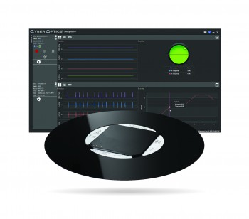
During SEMICON West, a thin, 3.5mm Auto Leveling and Vibration Sensor™ (AVLS3) in Chemically Hardened Glass (CHG) for smooth wafer handling and improved vacuum chucking will be introduced. It has a longer-range wireless capability and includes CyberSpectrum™ software that measures and reviews both applications simultaneously.
The front-end portfolio continues to grow. At CyberOptics, for example, 2018 revenues were up 23% year-over-year.
Inspection and Measurement in the Blending SMT and Semiconductor Markets
Companies such as CyberOptics are entering the merging SMT and semiconductor markets with new technology offerings. For example, CyberOptics is gaining significant traction in this market with its 3D Multi-Reflection Suppression (MRS) sensors. MRS-enabled sensors and systems revenues for 2018 were up 47% year-over-year.
There is an overlap in these two markets where there is an increasing need for 100% 2D & 3D inspection and measurement to identify critical defects and measure critical parameters. Customers want more than inspection and a pass/ fail report. They want X Y Z measurements to determine what it means for their process if the measurements are not right. They are considering what they feed back to their process and how they can control their process better.
Customers want high speed, accuracy and resolution. They need the best combination of these attributes for their applications. The 3D MRS sensor technology, for example, is highly valued for this combination, which is superior to any other 3D conventional technology. Key to the technology are the sophisticated algorithms that mitigate reflection-based measurement distortions for metrology-grade image quality. This is particularly vital for shiny surfaces and complex applications.
The 3D MRS-Enabled SQ3000™ Multi-Function system for AOI, SPI and coordinate measurements (CMM) continues to be rapidly adopted in SMT markets, particularly for high-end and challenging applications. Combined with the ultra high-resolution MRS sensor, it also is used for semiconductor applications. This multi-function, process control solution is unique in the market because the same system can identify critical defects and measure critical parameters.
MRS sensors are also incorporated into KLA® ’s back-end inspection systems.
Entering the Mid-End/ Advanced Packaging Market Where there is a Need for Speed
Leveraging the strength in SMT and back-end applications, CyberOptics is actively entering the mid-end area. In the semiconductor landscape, the mid-end is in between the front-end, where features are sub 10 μm, and the back-end, where features are typically greater than 100 μm.
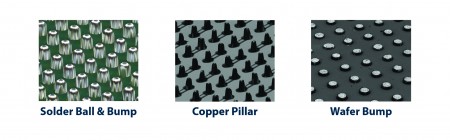
The mid-end and advanced packaging market is growing quickly. Within this market, there are flip-chip (FC), fan-in (FI), fan-out (FO), embedded die (ED) and TSV , all ripe for highly accurate 100% inspection. Stacked die, wire bonding, Cu pillars, C4 solder balls and bumps are some of the key applications (Figure 2). With all of the complexity, package varieties and continued advancements, yield challenges are increasing and there is a growing need to effectively identify and control defects.
For flip-chip IC, high-performance ICs such as FPGA, CPU, customers need 100% inspection to ensure quality. For advanced packaging, several bumped chips are often used, and if any bump fails, the whole package fails.
The industry currently requires high accuracy, high resolution and higher speeds for 100% inspection. Current 3D inspection technology is too slow for 100% inspection, so sampling inspection is being done. In addition, scanning twice, once for 2D and once for 3D, is time consuming. For example, current inspection methodologies for wafer bump metrology involve 3D bump height and bump coplanarity measurements and a separate scan for bump diameter and to measure location of bumps relative to nominal positions. Plus, increasing volumes amplifies the need for high speed.
Sensor Technology provides High Accuracy, Resolution and Speed
Sensor technology can provide numerous benefits, including accuracy, resolution and speed. Designed for the mid-end inspection area, for example, CyberOptics’ ultra-high-resolution three-micron 3D sensor delivers sub-micrometer accuracy that the industry needs for features that are as small as 25 μm. When first introduced in 2015, the MRS sensor technology’s pixel count was 18 μm. Over the last four years, however, it has advanced by a factor of six.
Additionally, the sensor now can handle mirror-like surfaces. While retaining its ability to reject spurious multiple reflections, the sensor can capture and analyze specular reflections from shiny surfaces of solder balls, bumps and pillars, enabling accurate inspection and 3D metrology of these critical packaging features.
Further, it is two to three times faster than alternate solutions in the marketplace. With data processing speeds in excess of 75 million 3D points per second, it delivers throughput greater than 25 wafers (300mm) per hour. Complete 100% 2D and 3D inspection can be accomplished at high speed for micro bump or pillar bump metrology, vs. the current practice of sampling a few dies of the 25 wafers.
Continued R&D Investment
To remain competitive in the semiconductor market, companies must continue to invest heavily in R & D. CyberOptics plans to advance the MRS sensor technology in terms of pixel size and advance the proprietary MRS algorithms, which will continue growing and strengthening its competitive advantage in the market.
Note: KLA is a registered trademark of KLA Corporation.


