ATS2
WaferSense® Auto Teaching System™ (ATS2)
Capture three dimensional offset data (x, y and z) to quickly teach wafer transfer positions.

Capture three dimensional offset data (x, y and z) to quickly teach wafer transfer positions.
Improve yields and lower particulate contamination with accurate wafer handoff calibration. ![]()
Achieve repeatable and reproducible semiconductor equipment setups. ![]()
Reduce equipment downtime from hours to minutes. ![]()
Speed trouble-shooting and lower consumable expense with visual inspection. ![]()
On-board image processor reports x-y-z offset from the teaching wafer to a target inside the equipment so you can teach wafer transfer coordinates.
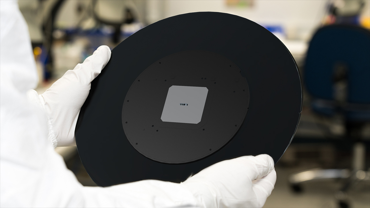

Wafer-shaped
Available in 200mm and 300mm wafer sizes.
Highly accurate
Accurate to +-0.1mm (+-0.004in) x and y position; +-0.8mm (+-0.03in) z position.
Wireless and vacuum compatible
Travels like a wafer and takes less time as equipment stays sealed during inspection. Transmits data in real-time.
Easy-to-use software
CyberSpectrum: Displays real-time video and measurements of target features, logs offsets and user comments. Allows teaching of circular features, 3mm-10mm diameter. Review functionality integrated; replays log file data for review and analysis.


