SAVE TIME. TAKE A BREAK

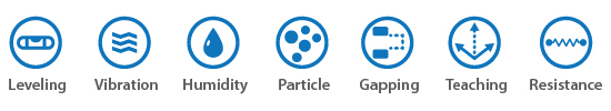
When you need the most efficient and effective measurement devices for semiconductor tool set-up and maintenance processes, count on CyberOptics, the global market leader in wireless semiconductor measurement devices for chamber gapping, leveling, wafer handoff teaching, vibration, airborne particle, relative humidity and resistance measurement.

Semiconductor fabs and OEMs value the accuracy, precision and versatility of the WaferSense and ReticleSense measurement portfolio to enable improvements in fab yields and equipment uptime.


Save Time & Expense

  • Improve yields and increase tool uptime
  • Increase throughput
  • Reduce resource needs
  • Speed equipment set-up, maintenance cycles, trouble-shooting, qualification and release to production
  • Speed tool optimization, stabilization and standardization
  • Streamline fab processes
  • Establish repeatable and verifiable standards
ATS

WaferSense® Auto Teaching System™ (ATS2)

  • Improve yields and lower particulate contamination with accurate wafer handoff calibration.
  • Achieve repeatable and reproducible semiconductor equipment setups.
  • Reduce equipment downtime from hours to minutes.
  • Speed trouble-shooting and lower consumable expense with visual inspection.
Learn More
ARS

WaferSense® Auto Resistance Sensor™ (ARS)

  • Shorten equipment maintenance cycles with wafer-like 4-wire resistance sensor.
  • Predict when a tool needs maintenance with quantitative analysis of measured mean resistance over time.
  • Improve cell-to-cell process uniformity with objective and repeatable resistance measurement.
  • Includes CyberSpectrum™ software.
Learn More
AVLS3

WaferSense® Auto Vibration and Leveling Sensor™ (AVLS3)

  • Speed equipment qualification with wireless measurements.
  • Shorten equipment maintenance cycles with thin and lightweight wafer-like form factor.
  • Lower equipment maintenance expenses and enhance process uniformity with objectiv eand reproducible data.
  • Includes CyberSpectrum™ Software
Learn More
APS1, 2 & 3

WaferSense® Airborne Particle Sensor™

  • Quickly monitors, identifies and enables troubleshooting of airborne particles down to 0.14um within semiconductor process equipment and automated material handling systems.
  • Easily identifies when and where the particles originate and measures the effectiveness of cleaning adjustments and repairs in real-time.
  • Includes CyberSpectrum™ software.
Learn More
AMS

WaferSense® Auto Multi Sensor™

  • Speed equipment qualification with wireless measurements.
  • Shorten equipment maintenance cycles with thin and lightweight wafer-like form factor.
  • Lower equipment maintenance expenses and enhance process uniformity with objective and reproducible data.
  • Includes CyberSpectrum™ software.
Learn More
AGS

WaferSense® Auto Gapping System™ (AGS)

  • Speeds non-contact gap measurements and parallelism adjustments under
    vacuum for semiconductor processes such as thin-film deposition, sputtering and etch.
  • Improves uniformity, tool availability and repeatability.
  • Includes CyberSpectrum™ software.
Learn More
AVS

WaferSense® Auto Vibration System™ (AVS)

  • Monitors 3-axis accelerations and vibration to enable yield improvements by maximizing acceleration and minimizing vibration.
  • Records vibration data for easy comparison between past and present, as well as one tool to another, to reduce particles, maintenance time and cycle time.
  • Includes CyberSpectrum™ software.
Learn More
ALS2V

WaferSense® Auto Leveling System 2 Vertical™ (ALS/ALS2V)

  • Speeds setting the right inclination by measuring pitch, roll, rise overrun and vertical inclinations.
  • Quickly and accurately enables setting the same level across the tools for better process uniformity.
  • Includes CyberSpectrum™ software.
Learn More