 Back to News
Time-Resolved, In-Line Airborne Particle Sensing Pinpoints Contamination Sources for Faster Recovery and Lower Risk to WIP
V. Vijay, CyberOptics Corporation

As featured in Semiconductor Digest’s August/ September 2021 Edition. View the digital magazine on Semiconductor Digest.
Fine particles (less than 5 micrometers in diameter) can have a disastrous impact on semiconductor manufacturing. From the earliest days, manufacturing facilities have deployed air filtering and recirculation to remove particles from the cleanroom, but particles may still be generated inside process tools, where they can cause defects and yield loss. Quickly identifying when and where airborne particles originate can be challenging, but it is critical to success. Conventional methods for monitoring and diagnosing contamination problems take considerable time to return results. Because of their intermittent nature, they are not good at detecting precisely when within the process cycle contamination appears, or at issuing immediate real-time alerts. As a result, contamination episodes are often not seen until defects are detected by downstream inspections. In-line particle sensing (IPS™) provides continuous, immediate, time-resolved monitoring that can shorten response times, protect work-in-progress, and facilitate root cause analysis.
During the manufacturing process, semiconductor devices are extremely vulnerable to defects caused by particulate contamination. Manufacturers go to great lengths to prevent contamination. The process takes place in a cleanroom, where air is constantly recirculated and filtered to remove particles. Even within the cleanroom, when wafers are transported from tool to tool, they are enclosed in specially designed air-tight containers and never exposed the ambient environment. However, contaminants generated inside process tools can still cause defects and yield loss, and engineers carefully monitor tools to detect contamination. Most monitoring relies on the inspection of monitor wafers, which are run through the process tool routinely, or in response to a contamination problem detected by downstream inspection of product wafers. This approach has shortcomings. It is not continuous and may miss an event that occurs between samples. It takes tool-time to run monitor wafers that could be used to process product wafers. It is slow, taking considerable time to return results and meanwhile putting additional wafers at risk. It is not time resolved, making it difficult to know when in the process cycle the contamination appeared. A new in-line particle sensor addresses these shortcomings. It can be installed in the process chamber exhaust line, where it can provide continuous, time-resolved monitoring of all gas flowing out of the chamber, detecting particles larger than 0.1μm.
EUV lithography is especially vulnerable to particulate contamination for several reasons. It is used to create the smallest structures in the circuit, where even the smallest particle can result in a killer defect. It is a bottleneck process – every layer begins with lithography, when it stops, the whole process stops. Moreover, EUV systems are capital intensive. Earning an adequate return on that substantial investment requires the system to operate constantly at maximum throughput with little or no downtime. For these reasons, maintaining system availability has the highest priority. Any time saved by early detection and rapid response to process excursions or contamination events is extremely valuable. Maximizing yield and tool uptime in photolithography processes requires best-in-class practices to achieve a contamination-free process environment. Unfortunately, identifying precisely when and where airborne particles originate is challenging with traditional methods.
There are three widely used methods for particle detection in photolithography systems: bench-top & hand-held airborne particle counters, monitor reticles (analogous to monitor wafers), and in-situ particle scanners. All three of these traditional methods have substantial drawbacks:
• Bench-top counters require long hoses to reach into the tool—and are often incapable of following the reticle path. Similarly, bench-top and handheld methods make it difficult (often impossible) to reach all locations of interest. In some cases, equipment engineers must crawl through the scanner to make accurate measurements, adding an additional contamination risk from the measurement itself.
• Monitor reticle scanning is time-consuming, creating long delays for test results. The process has many steps and typically involves considerable waiting for tool availability and lost tool time while the tool executes non-productive test cycles: 1) premeasure the test reticle, 2) load the test reticle into the tool, 3) put the test reticle through a normal operational cycle, 4) Remove the test reticle and wait for inspection tool availability, 5) perform the post measurement, 6) analyze results. If problems are found, repeat the measurement process. Monitor reticle scanning does not deliver time resolved results and cannot determine precisely when and where the reticle became contaminated.
• In-situ scanners are usually separate from the tool and look at particles deposited on a wafer not in the air. They are good at identifying particles but limited in their ability to pinpoint when and where in the wafer handling process the particles accumulated on the wafer. Like monitor reticles, they do not provide time-resolved data or timely alerts, which could prompt proactive intervention to avoid contamination of product wafers.
These issues have driven the development of a sensor that can detect airborne particles in vacuum and gas flow lines – the In-line Particle Sensor™ (IPS™, CyberOptics Corporation) shown in figure 1. IPS mounts permanently on a supply or exhaust line and detects particles 24/7. It can detect particles of 0.1micron size and higher. Its 10-6 Torr operating range allows installation of the IPS on any vacuum line, where it can detect any particles that pass through its interaction region without risk of leakage. Although its design targets pressure ranges typical of chamber exhaust lines, where substantial gas flows move particles at relatively high speeds, it can also be used in high-vacuum lines where particles move more slowly.
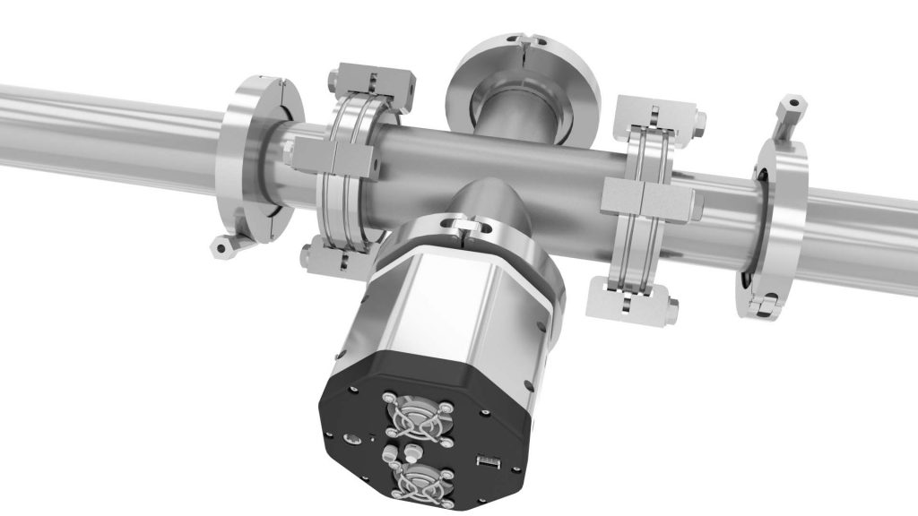
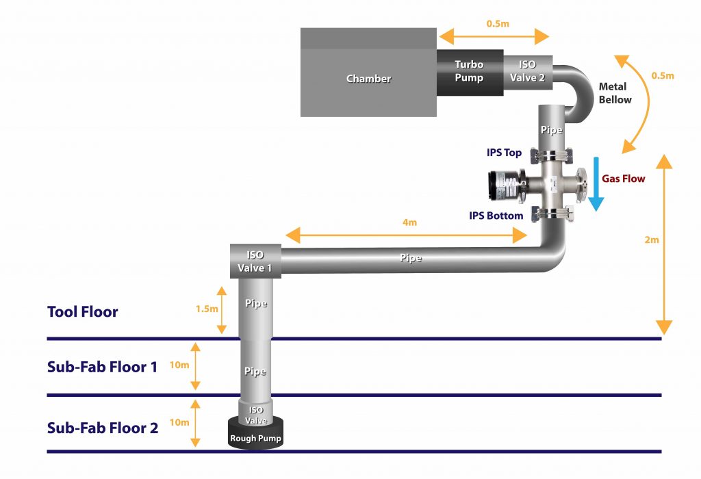
Figure 1. (left) IPS particle sensor, (right) the IPS is normally installed in the process exhaust stream, in this example just after the exit port of the turbo pump mounted on the chamber.
The particle stream travels through the sensor in a straight line and a light source and sensing optics are configured along an orthogonal axis in the crossing arm of a vacuum fitting. When a particle passes through the laser beam in the area in front of the IPS sensor head, the particle scatters some of the laser light. That light is collected by an optical system and sensed by a photodiode. The particle sensing and analysis occurs on a microsecond time scale. Processing takes place in the sensor, and the information is transmitted via Bluetooth link to the host computer, where it is displayed in real time. A software application (CyberSpectrum™, CyberOptics Corporation) manages data display, analysis, and storage.
Collisions between gas molecules and particles move the particles in the direction of the gas flow. Since the IPS is primarily intended for use in vacuum forelines, the pressure in the IPS sensing area is relatively low and gas flows much faster than any particles, often orders of magnitude faster. At very low pressures, (high vacuum) particles may flow very slowly because there are very few gas-particle collisions. Particle velocity therefore depends on pressure, gas flow velocity, residual gas type, particle size, and other factors. Electronic filtering in the IPS allows very slow particles to be sensed.
Experience has shown that most particle “events” occur when the process chamber pressure is changing or when system components or product wafers are moving inside the system. Continuous, time-resolved, in-line particle sensing with the IPS has demonstrated a clear advantage in locating and troubleshooting airborne particles in photolithography environments. By recording particle counts versus time, particle generating events can be precisely correlated with process events occurring inside the tool. The software graphically displays particle events over time as they occur and stores them in various formats for later analysis. EUV customers have shown clear correlation between IPS measurements and particle adder events
The laser based counting technology of the IPS can also be incorporated in physical formats that mimic the form factors of wafers or reticles (figure 2). With these sensors, measurements are both time-resolved and location specific, allowing engineers to determine when and where contamination is detected as the counter transits the process tool. The wireless sensors count particles, bin them as large (>0.5µm) or small (>0.14µm) and communicate with a host PC over a Bluetooth link. They include active airflow to draw sampled gas and particles through the sensor. The system records data for analysis and permanent maintenance records, ensuring appropriate follow-up. These sensors can be used in existing tools with no additional hardware or modifications.
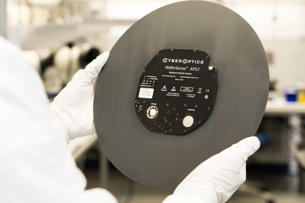
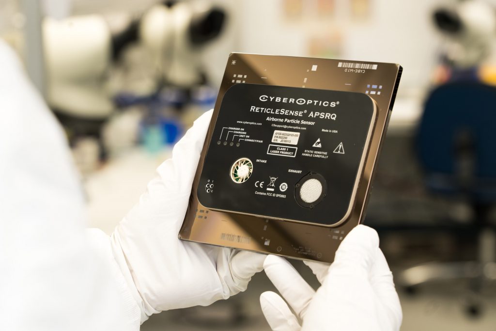
Figure 2. The same particle counting technology used in the IPS can be incorporated in formats that mimic wafer or reticle geometry. These sensors help to localize particles sources as the sensor passes through the process tool.
Table 1 compares the steps and time required for monitor reticle and wireless particle counting techniques. Monitor reticles do not deliver time-resolved results, making it difficult to determine precisely when and where the contamination occurred. Wireless particle detection checks the entire reticle path inside the tool and is 10 times faster.
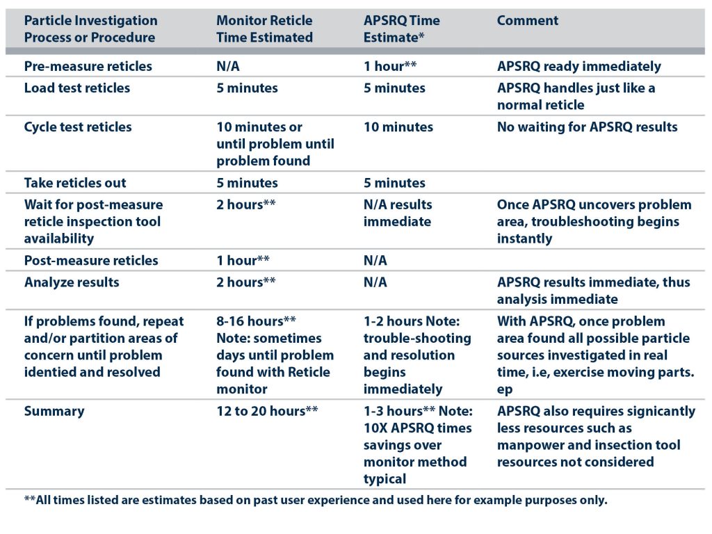
Table 1. The table compares monitor reticle and reticle-format wireless particle sensing.
Results
An IPS was installed on an EUV photolithography system, located in the vacuum exhaust line just after the turbo pump that evacuates the process chamber. In this configuration any particles generated in the system are concentrated and conveyed through the IPS in the turbo pump exhaust stream.
In the first example, the IPS collected data continuously for over a month (figure 3). Particle counts began to increase steadily within a few days of installation, indicating a process issue. An investigation revealed the source. A technician performed the required maintenance and returned the tool to nominal performance. Early detection, and the proactive corrective action it enabled, prevented yield loss, and saved time and money.
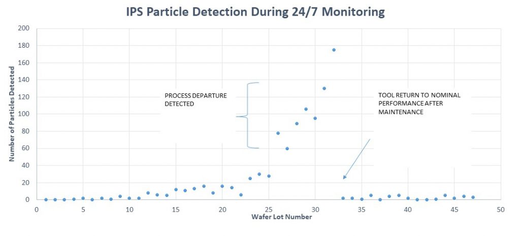
Figure 3. Installed on an EUV Lithography system, the IPS detected a significant increase in particle counts a few days after installation, indicating a need for intervention. Service personnel performed maintenance and the particle levels returned to normal.
The data in the following two plots were collected by an IPS monitoring particle counts during N2 purge cycles of a PVD process tool. The tool manufacturer wanted to confirm the efficacy and determine the efficiency of the purge for eliminating particulate contaminants. Figure 4 shows time-resolved data collected during the purge as the particle count spikes and returns to zero over a period of less than a minute. The solid line is instantaneous count rate, the dashed line is average count rate, and the dotted line is pressure. Figure 5 shows data from the same tool monitored continuously over a period of 20 hours and including multiple purge cycles. The time-resolving capabilities of the IPS are essential in correlating particle counts with specific events in the process cycles to identify contamination sources.
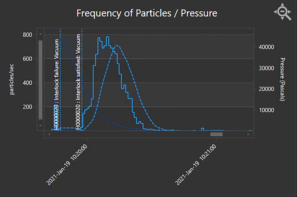
Figure 4. Time-resolved data collected by an IPS during a N2 purge cycle. Over a period less than a minute, pressure (dotted line) spikes first, followed by particle counts (instantaneous – solid line, average – dotted line) as the gas moves the particles through the system. (The interlock messages refer to safety provision that prevent the sensor’s laser from turning on until appropriate conditions are achieved.)
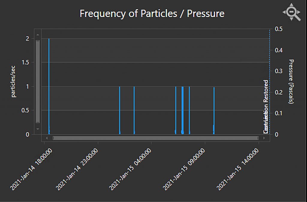
Figure 5. The same system as figure 4, monitored continuously over a period of 20 hours that included multiple purge cycles.
Conclusion
The need to maximize process yield and tool availability drives requirements to control particulate contamination within process tools as well as within the cleanroom. Conventional methods for particle detection are not fast enough to provide time-resolved measurements or support real-time alerts of contamination. IPS and wireless wafer/reticle format counters can detect particulate contamination events exactly when and where they occur, with results available in real-time, or stored for later analysis. IPS mounts permanently in the supply or exhaust line and delivers continuous monitoring. Wireless wafer/reticle-format sensors travel through process tools, allowing them to pinpoint the contamination source within the tool. Rapid results permit faster determination of root causes and shorten repair/maintenance cycles. Real-time monitoring supports proactive maintenance, potentially eliminating unplanned downtime events and consequential damage to work-in-progress.
Acknowledgements
Portions of this work were previously described in the proceedings of SPIE’s Photomask Japan 2021 (DOI 10.1117/12.2613075) and are included here with permission.


