 Back to News
CyberOptics Showcases Yield-Improving Sensor Technology Solutions at Semicon Europa
Minneapolis, Minnesota— November 5, 2021 — CyberOptics® Corporation (NASDAQ: CYBE), a leading global developer and manufacturer of high-precision 3D sensing technology solutions will feature the In-Line Particle Sensor™ (IPS™) and Auto Resistance Sensor™ (ARS™) for semiconductor tool set-up and equipment diagnostics at Semicon Europa in Munich, Germany, from November 16-19th in booth B1101. The company will also feature the WX3000™ Metrology and Inspection system for wafer-level and advanced packaging.
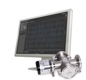
Cyberoptics’ In-Line Particle Sensor (IPS) with CyberSpectrum™ software detects particles in gas and vacuum lines 24/7 in semiconductor process equipment and other controlled environments. It is particularly relevant for EUVL tools where the ability to monitor particles in-line can significantly improve EUVL tool yield and productivity. An extension of the industry-leading WaferSense® Airborne Particle Sensor™ (APS™) technology that is documented by fabs as the Best-Known Method (BKM), the IPS quickly identifies, monitors and enables troubleshooting of particles down to 0.1µm. The effects of cleaning, adjustments and repairs can be seen in real-time.
CyberOptics will demonstrate the WaferSense® Auto Resistance Sensor™ (ARS) for semiconductor tool set-up and diagnostics. The 300mm Auto Resistance Sensor (ARS) with CyberSpectrum software enables real-time resistance measurements to detect residue affecting plating pins in semiconductor Electrochemical Deposition (ECD) applications. Process and equipment engineers in semiconductor fabs can predict when a tool needs maintenance with quantitative analysis of measured mean resistance over time, shorten equipment maintenance cycles, and improve cell-to-cell uniformity with the wafer-like, 4-wire resistance sensor.
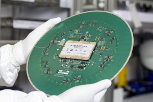
The company also will feature the CyberOptics’ WX3000™ system powered by the 3 µm NanoResolution Multi-Reflection Suppression™ (MRS™) sensor that provides sub-micrometer accuracy on features as small as 25µm. While retaining its ability to reject spurious multiple reflections, it adds the ability to capture and analyze specular reflections from shiny surfaces of solder balls, bumps and pillars, allowing highly accurate inspection and metrology of these critical packaging features. Fast, 100% 3D/2D inspection and metrology can be conducted with throughput greater than 25 wafers (300mm) per hour, 2-3X faster than alternative solutions.


