Back to News
Measuring bump height uniformity to improve yield using 3D inspection

Read our latest technical article published in Chip Scale Review.
Measuring bump height uniformity to improve yield using 3D inspection
By Tim Skunes, Vice President of Research and Development
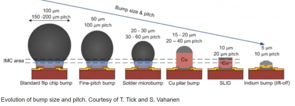
Chip -scale wafer-level packaging (WLP) offers important benefits— small package size and the ability to process hundreds or thousands of dies in parallel. A variety of bump configurations are possible, depending on the application, as shown in Figure 1 [1]. One challenge with WLP is maintaining uniformity of solder bumps or copper pillars across a 300mm wafer. Metrology and inspection are necessary to ensure device reliability. Shrinking bump heights and spacing and high aspect ratios, however, make wafer-level bump height inspection especially challenging. It is also increasingly critical because minor variations in bump height across a wafer can reduce overall yield. Defects related to bumping can affect both thermal and electrical device performance [2].
It can be tempting to cut down on the number of inspection steps or only test a sample of wafers coming through the line. Doing so can speed up production. For legacy processes where the yield is high, a partial inspection may be the best approach. When design rules change and yield drops, it becomes apparent that reducing inspection does not save time in the long run. The best way to improve yield, especially for a new process, is to identify defects early. That often requires 100% inspection
across each wafer in every batch. Stringent inspection protocols help identify the root cause of defects and reduce the need to rework or scrap wafers.
Existing bump height measurement methods have two drawbacks: speed and placement in the process flow. They slow down production and often do not catch defects early enough in the process. While 100% inspection is commonplace during process development, it is often abandoned for high-volume production because of the time required for testing. Fast, accurate metrology and inspection are the key to success. This article explains the benefits of 3D fringe projection technology to inspect solder bumps and copper pillars at the wafer level, comparing it to conventional approaches for bump height measurement.
Conventional bump height measurement
Pillar bumps consist of three layers: a copper pillar, a nickel barrier layer, and a tin/silver/copper (SAC) solder bump. Bump height measurements are typically taken after the final photoresist stripping step, as shown in Figure 2. This occurs after all three layers of the bump have been deposited.
Conventional noncontact bump height measurement relies on line scan triangulation. An incident beam of laser or white light deflects off the object being measured. With line scan triangulation, the light source projects a line onto the object. A detector with an array of photosensors captures the reflection and calculates the distance. Scanning across a wafer produces a map of bump height data. Line scan triangulation has two primary drawbacks. One of these is speed. A 300mm wafer can contain hundreds of millions of copper micro bumps [3], and 100% inspection is not economical.
The other drawback to line scan triangulation is that it happens too late in the manufacturing process. Inconsistent copper plating is often