Back to News
New Wafer-Like and Reticle-like Sensors Deliver Fast, Easy Measurements Inside the Process Chamber: WaferSense® ATS2 and ReticleSense® ATSR Case Study
As appears in the July 2022 Issue of Semiconductor Digest.
An excerpt from the case study:
Teaching Sensors
Teaching sensors are used to monitor and tune the accuracy of wafer and reticle handling operations. They use cameras that are accurately located with respect to the edges and surfaces of the wafer- or reticle-like substrate to evaluate the position of the sensor relative to visible references, such as a mark indicating the center of a chuck. They can quickly report offset values to monitor accuracy or provide data for training/fine tuning robot transfers. They eliminate operator-induced variability from the measurement. Their radio communication and vacuum compatibility allow the tool to remain sealed throughout the measurement, often reducing equipment downtime from hours to minutes. The camera can also be used for inspection and other tasks, such a searching for lost wafers or verifying that a pedestal is free of debris, without opening the tool.
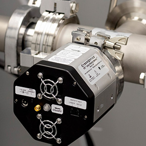
New wafer-like teaching sensor
A new wafer-like teaching sensor (CyberOptics ATS2 – Figure 3) expands on the capabilities of previous sensors. Notably, it has cameras on both the top and bottom surfaces. Both cameras are high resolution color cameras with white light illumination, and a faster video imaging rate. The upward looking camera provides inspection and measurement of components above the sensor, such as showerheads and photoresist dispensing nozzles. The sensor is thinner, for compatibility with more systems, and has a smoother bottom surface for better vacuum chucking. It provides more accurate offset measurements and can handle more complex alignment mark shapes.
In use, the sensor relies on the accurate positioning of the camera with respect to its wafer-like outline. This establishes an X-Y coordinate system, with the X direction defined by a notch in the sensor edge. For accurate measurements, the operator must ensure the sensor is positioned on the robot in the same way a wafer would be, and the notch is properly oriented. The scale of the coordinate system projected on the surface where the alignment mark is located is determined by a simple geometric relationship that requires accurate knowledge of the working distance between the camera and the surface. This can be supplied by the operator or calculated by the sensor based on measurements of a feature of known size on the alignment surface.
Visit Semiconductor Digest to read the full case-study.