 Back to News
SQ3000 for SPI Featured in Mycronic Case Study
As published in IConnect007 article “Solder Paste Jetting: An Integral Approach”| Jeff Leal, Gustaf Mårtensson, and Nerijus Augustis, Mycronic ABRead full article at IConnect007
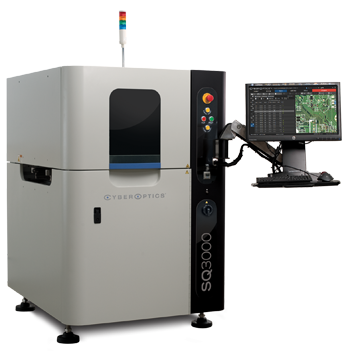
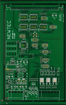
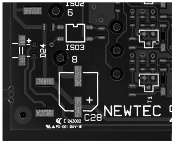
In a recent article published on IConnect007, CyberOptics’ SQ3000 for AOI/ SPI system was used to scan and obtain images of 400 PCB panels distributed over two different layouts in a test series to analyze solder paste jetting deposits to detect deposit quality on each pad pattern.
Jetting solder paste is a technique where the mechanics differ greatly from traditional solder paste deposition methods.
Jet Printing Solder Paste
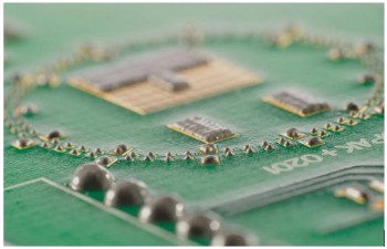
In general, jet printing is the transfer of momentum from a piston to the material—in this case, solder paste. Jetting on the fly is the capability of jetting material without stopping the gantry system, which enables the highest possible throughput. The most common form of jetting requires direct contact of the piston with a seat to transfer momentum. Due to the softness of the solder particles in the paste, this method is inadequate because it leads to flattening of the spheres (referred to as “coining”) and eventually clogging the nozzle orifice.
To jet solder paste reliably, the transfer of momentum must be made without contacting a hard surface to eliminate the coining effect, thus resulting in continuous jetting over time. The best method of transferring momentum without contact is through very high accelerations, coupling high accelerations with precise volumetric control enables the jetting of a wide range of dot sizes with a single hardware setup.
Methodology
The test series encompassed approximately 400 PCB panels distributed over two different layouts. All boards were produced using one of two Mycronic MY600 jet printers with two V49 ejectors for the actual deposition of solder paste. The solder paste used in the trial was the Senju LFAC19 (from Senju Metal Industry Company Ltd). A total of 45 cm3 of solder paste was consumed during the test. After each case of jetting of any PCB on the MY600, each panel was scanned by a CyberOptics SQ3000, a 3D AOI machine from CyberOptics Corporation to obtain images of the jetted deposits to detect deposit quality on each pad pattern.
Read full article at IConnect007


