 Back to News
Extending 3D MRS Technology to Address Challenging Measurement and Inspection Applications
John Hoffman, PhD, Senior Image Process Research Engineer at CyberOptics, will present the paper ‘Extending the 3D MRS Technology to Address Challenging Measurement and Inspection Applications.’ CyberOptics will participate in a technical session focused on Multi-Reflection Suppression (MRS) sensor applications at SMTA International at the Donald E. Stevens Convention Center in Rosemont, Ill on Thursday, Oct. 18, 2018.
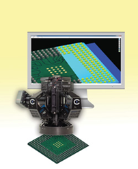
There is an increasing need for highly accurate 3D inspection and measurement capabilities for various challenging applications in SMT, semiconductor and metrology markets. 3D Multiple Reflection Suppression (MRS) sensor technology has been effectively used for 3D Automated Optical Inspection (AOI) for several years and is now effectively being utilized for 3D Solder Paste Inspection (SPI) applications such as microelectronics and sub-100 micron solder paste deposits and other challenging applications such as semiconductor packaging, socket metrology, automotive, medical and others with stringent requirements.
In addition to inspection, there is an increasing need to capture coordinate measurements in-line. MRS sensors can attain highly accurate measurements in seconds compared to hours with traditional Coordinate Measurement Machines (CMMs). MRS sensor technology provides significant advantages in speed, accuracy and resolution over alternate technologies.
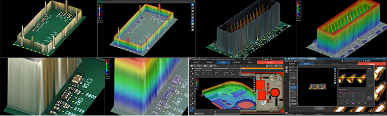
Using multi-view 3D sensors and parallel projection, it is possible to capture more of the assembly or object at a faster rate as compared to serial image acquisition, which is more time consuming. Precise 3D image representation can then be generated using sophisticated fusing algorithms that take the multiple captured images and fuse them into one precise 3D image. The result is highly accurate, high speed 3D inspection.
Multi-reflection suppression (MRS) technology enables highly accurate 3D measurement by meticulously identifying and rejecting reflections caused by shiny components and reflective solder joints. MRS algorithms use a very rich data set from multiple cameras at every location. Combined with sophisticated algorithms that fuse the image data from multiple cameras, multiple reflections are effectively suppressed.
MRS sensor excels in accuracy, resolution and speed for various challenging applications. For example:
Automated optical inspection and measurement for tall components, small components in the shadow of tall components and shiny components and processes.
Solder paste inspection, microelectronics and sub-100 micron solder paste deposits, very small LEDs – mini LEDs, micro LEDs, as well as paste printing onto chip products.
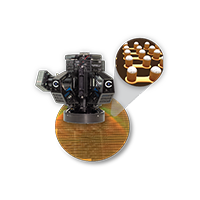
Metrology for various machined and molded parts, to socket metrology.
Semiconductor inspection and measurement in both the back-end and mid-end for IC- packaging, wafer bump inspection other semiconductor applications.
Flux inspection, wire bond inspection, dye-attached applications, shiny flip chip packaging and more.


