Back to News
CyberOptics to Present ‘High Precision Sensing Technology for Semiconductor Inspection and Measurement’ at SEMICON West
CyberOptics® Corporation (NASDAQ: CYBE), a leading global developer and manufacturer of high-precision 3D sensing technology solutions, will present at SEMICON West, at the Moscone Center in San Francisco, CA on July 10 in the North Hall E, Room 20 at 11:15am. The company will also exhibit at the show in booth #5769.
Tim Skunes, VP of R&D at CyberOptics, will present the technical paper ‘High precision sensing technology for semiconductor inspection and measurement applications.’ The semiconductor packaging industry continues to advance, with new designs adding more layers, finer features and more I/O channels for higher bandwidth and lower power consumption. In addition to the increased complexity, shiny and mirror-like surfaces present inspection challenges.
For mid-end and advanced packaging inspection and measurement, CyberOptics will demonstrate the new proprietary NanoResolution Multi-Reflection Suppression (MRS) sensor technology that meticulously identifies and rejects multiple reflections caused by shiny components and mirror-like features. Effective suppression of multiple reflections is critical for highly accurate measurements.
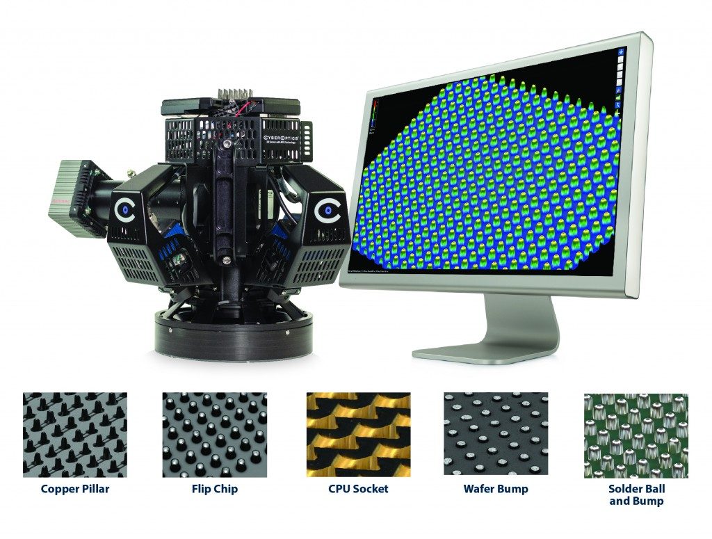
Offering an unparalleled combination of high accuracy, high resolution and speed, MRS sensors are widely used for inspection and measurement in the SMT, semiconductor and metrology markets. The new 3- micron NanoResolution MRS sensor enables metrology grade accuracy with superior 100% 2D and 3D inspection performance for features as small as 25-micron.
Further, it is two to three times faster than alternate solutions in the marketplace. With data processing speeds in excess of 75 million 3D points per second, the NanoResolution MRS sensor delivers throughput greater than 25 wafers (300mm) per hour. 100% 2D and 3D inspection can be completed simultaneously at high speed, versus an alternate, slow method that requires two separate scans for 2D and 3D, and only a sampling of a few dies of the 25 wafers.
This best-in-class MRS sensor technology is ideally suited for the inspection of CPU sockets, IC package, solder balls and bumps, copper pillars, and other advanced packaging and mid-end semiconductor applications where high precision and speed are needed to improve yields, throughput and process control.