Back to News
SMTA International With Dr. Subodh Kulkarni
NJ: Hi, Nolan Johnson here for RealTime with SMTAI and I’m speaking with CyberOptics’ President and CEO, Dr. Subodh Kulkarni. Subodh, welcome.
SK: Thanks, Nolan, how are you?
NJ: I am terrific. We’re discussing SMTAI and you have some new product technology on the show floor here. Tell me about it.
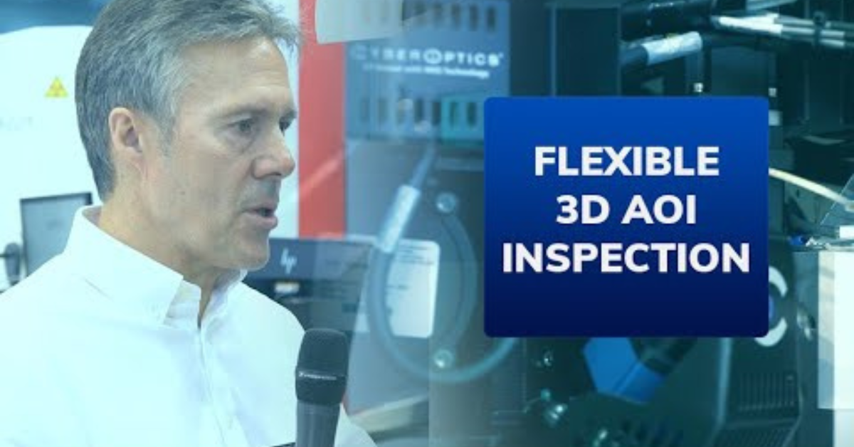
SK: Sure, we are excited to launch two new products at the SMTAI show. One is what we call SQ3000+™, it’s the latest of our SQ3000™ Multifunction for SPI, AOI, CMM family of products. This one is unique in the way we have maintained the speed, high accuracy and high resolution of SQ3000, but we have significantly improved the resolution. The new system is at a 5-micron resolution.
But, in addition to the higher resolution, we have also enabled the system to handle extremely shiny parts, very reflective soldering joints or silicon wafers, or copper pillars, and those kinds of very shiny objects that most AOI systems on the show floor struggle in measuring and inspecting. So, we are pretty pleased with that significant advancement that we are bringing to the show floor.
In addition to the SQ3000+, we are also launching the WX3000™ system, that’s again like SQ3000+, it’s based on our proprietary MRS™ technology, MRS stands for Multi-Reflection Suppression™, meaning we are doing 3D noncontact optical sensing that enables higher speed and resolution.
In the WX3000 system, we do have a very unique sensory geometry, multiple projectors, multiple cameras, that can enable metrology and inspection of extremely shiny objects like bumps on silicon wafers at a very, very high resolution. The WX3000 is a 3-micron resolution, it’s even higher resolution than the SQ3000+, specifically for the backend semiconductor applications like bumps and pillar inspections on wafers. So, we’re pretty excited to have those two advancements at the show.
NJ: Given what you are talking about here, Subodh, I have to ask, are you seeing some convergence between PCB applications and semiconductor applications? It would seem from these two products that you are.
SK: Absolutely, Nolan, you are right on, and clearly in our technology platform, you can see that we are deploying the same MRS sensor technology to enable both SMT and semiconductor applications. And the reason for that is there is a very significant convergence between the two markets. Historically the PCB manufacturing and inspection market were very different than the backend of the semiconductor market, but increasingly, if you look at modern electronics, like the latest IPhone® or other advanced electronic products you will notice that the traditional PCB does not look like a traditional PCB anymore. It is really a bunch of advanced modules and packages that are strung together. And we’re seeing convergence across the board.
So, companies that historically dealt with only backend semiconductor are beginning to do more and more SMT-like applications and vice versa. Many SMT companies are shifting their focus to wafer-like devices in their processes and inspections. So, we definitely see a convergence going on between SMT and semiconductor and we are very much in that convergence.
NJ: You know, Subodh, as I listen to you, this sounds a whole lot like the heterogenous integration technology that’s been talked about a lot. Does that fit in with where you’re headed?
SK: Absolutely, heterogeneous integration, stacking of chips, there are many things that are driving this convergence, but definitely there is a commonality here that is going across the two industries that are forcing the convergence.
NJ: Not to get you to spill secrets too much, but what can we expect to see in the next year or two in this space from CyberOptics?
SK: Well, as you know, it’s an unusually interesting time in both semiconductor and electronics. There is a significant surge in demand for both chips, as well as high-end electronics. The pandemic may not have shifted any fundamental trends, but it certainly accelerated the trends that were already in place. It’s hard to avoid headlines these days without seeing the shortage of semiconductor chips and electronic devices right now.
So, that significant demand is spurring a lot of investment, and it’s an exciting time to be in this industry. A lot of new FABs are being built, a lot of new lines are being placed to meet this surge in demand. So, in that context, we are trying to keep up with demand. Demand is extremely high right now.
But in addition to the complexity, when new capital is being deployed, companies want to put in the latest and best, they don’t want to put one generation or two-generation old things. The demand for high-end electronics inspection and metrology systems that are needed to do those has increased rapidly, so we expect to continue to improve the sensor resolution further and we expect to continue to improve the speed further. The need is growing even more rapidly now with such a high demand for chips. So, I hate to sound boring, but we’ll continue with kind of the same except at a faster rate, and faster, better kind of stuff.
NJ: Well, thank you very much for the update, very insightful, as always.
SK: Thank you, Nolan.
NJ: Here at SMTAI for RealTime With SMTAI, I’m Nolan Johnson. Thanks for listening.