 Back to News
CyberOptics to Unveil New Teaching System for Semiconductor Applications at SPIE Photomask Technology and EUV Lithography
CyberOptics® Corporation (NASDAQ: CYBE), a leading global developer and manufacturer of high-precision 3D sensing technology solutions, will exhibit at the SPIE Photomask Technology and Extreme Ultraviolet Lithography conference from September 27-28th at the Monterey Conference Center in California.
CyberOptics® Corporation (NASDAQ: CYBE), a leading global developer and manufacturer of high-precision 3D sensing technology solutions, will exhibit at the SPIE Photomask Technology and Extreme Ultraviolet Lithography conference from September 27-28th at the Monterey Conference Center in California. The company will unveil the new ReticleSense® Auto Teaching System™ (ATSR™) and showcase the In-Line Particle Sensor™ (IPS™) among other devices.
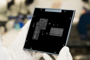
The new ReticleSense® ATSR is a multi camera sensor used with CyberSpectrum™ software to teach accurate reticle hand-off calibration for proper alignment and set-up of semiconductor tools. The sensor “sees” inside to capture three dimensional off-set data (x, y and z) in real-time to quickly teach reticle transfer positions – all without opening the tool. Process and equipment engineers can conduct repeatable and reproducible setup and maintenance checks, speed trouble-shooting and eliminate technician-to-technician variation.
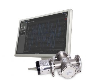
The company will also display an extension of the industry-leading WaferSense® and ReticleSense® Airborne Particle Sensor (APS) technology that is documented by fabs as the Best Known Method (BKM). The In-Line Particle Sensor (IPS) with CyberSpectrum™ software detects particles in gas and vacuum lines 24/7 down to 0.1μm. The sensor is particularly relevant for EUVL tools where the ability to monitor particles in-line can significantly improve tool yield and productivity.


