 Back to News
CyberOptics Demonstrates Advanced Sensor Technology at SEMICON Taiwan
Sensors save time, save expense and improve yields in semiconductor fabs
Minneapolis, Minnesota— September 2, 2020 — CyberOptics® Corporation (NASDAQ: CYBE), a leading global developer and manufacturer of high-precision 3D sensing technology solutions, will exhibit at SEMICON Taiwan, September 23-25 in booth #L0310. During the show, the company will feature its new In-Line Particle Sensor™ (IPS) and Auto Resistance Sensor™ (ARS) for semiconductor tool set-up and equipment diagnostics, and the WX3000™ Metrology and Inspection system for wafer-level and advanced packaging applications.
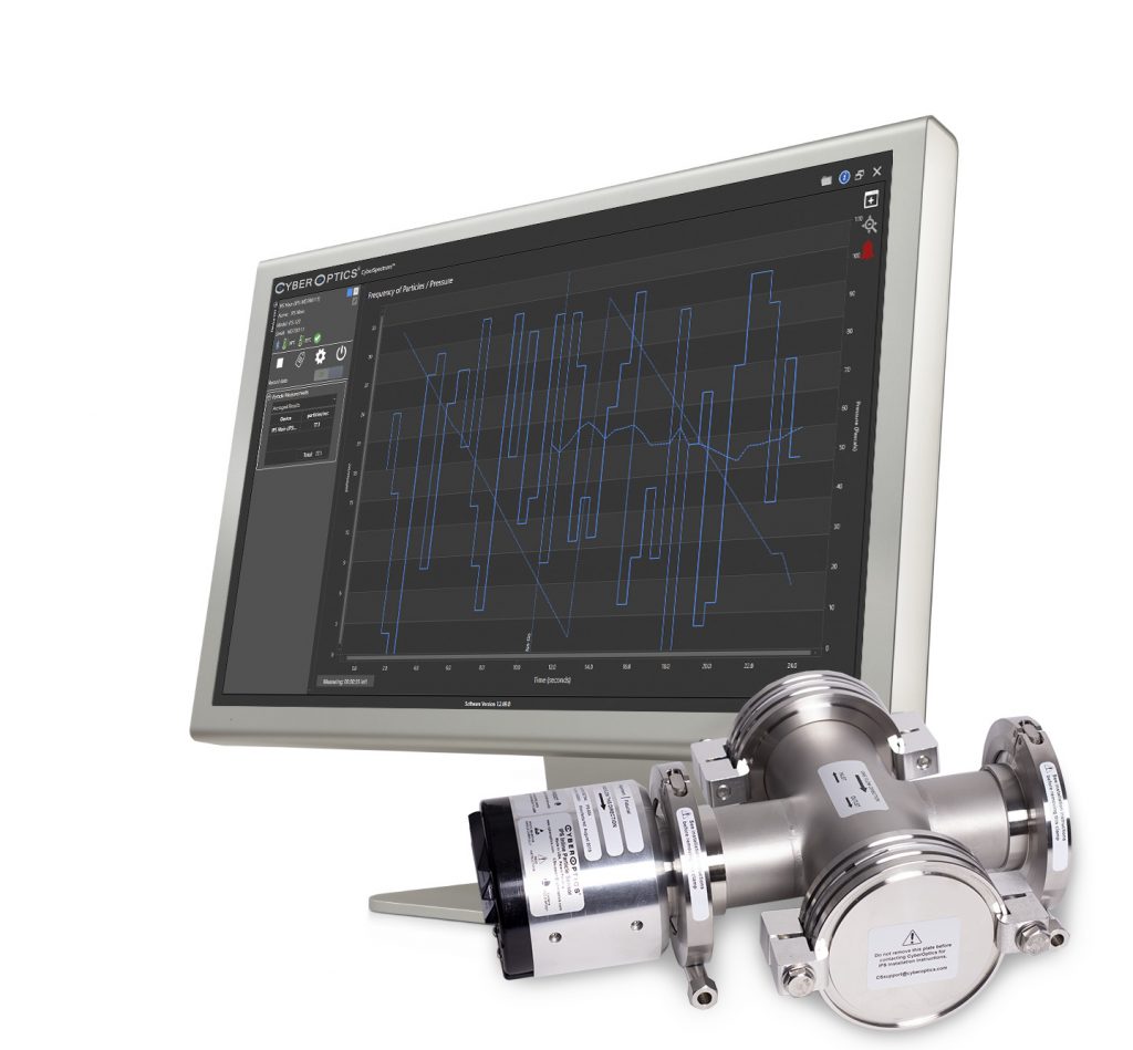
An extension of the industry-leading WaferSense® and ReticleSense® Airborne Particle Sensor (APS) technology that is documented by fabs as the Best Known Method (BKM), the new In-Line Particle Sensor (IPS) with CyberSpectrum™ software detects particles in gas and vacuum lines 24/7 in semiconductor process equipment. The IPS quickly identifies monitors and enables troubleshooting of particles down to 0.1µm.

The new WaferSense® Auto Resistance Sensor™ (ARS) with CyberSpectrum™ software for semiconductor tool set-up and diagnostics enables real-time resistance measurements of plating cell contacts in semiconductor Electrochemical Deposition (ECD) applications.
Process and equipment engineers in semiconductor fabs can speed equipment qualification, shorten equipment maintenance cycles, lower equipment expenses and optimize preventative maintenance plans.
“Whether it’s used in the front-end, mid-end or back-end of the semiconductor fab, our high-precision sensor technology is delivering significant improvements in yields, processes, productivity and through-put,” said Dr. Subodh Kulkarni, President and CEO, CyberOptics.
For wafer-level and advanced packaging metrology and inspection, the new WX3000™ system will be featured. Performing two to three times faster than alternate technologies at data processing speeds in excess of 75 million 3D data points per second, the NanoResolution Multi-Reflection Suppression™ (MRS™) sensor-enabled WX3000 systems deliver throughput greater than 25 wafers per hour. 100% 3D and 2D metrology and inspection can be completed simultaneously at high speed, as compared to an alternate, slow method that requires two separate scans for 3D and 2D and only a sampling of a few die.
The proprietary NanoResolution MRS sensor, deemed best in class, meticulously identifies and rejects multiple reflections caused by shiny and mirror-like surfaces. Effective suppression of multiple reflections is critical for highly accurate measurements.


